- 您现在的位置:买卖IC网 > Sheet目录1993 > DS1123LE-100+ (Maxim Integrated Products)IC DELAY LINE 256TAP 16-TSSOP
DS1123L
3.3V, 8-Bit, Programmable Timing Element
6
______________________________________________________________________
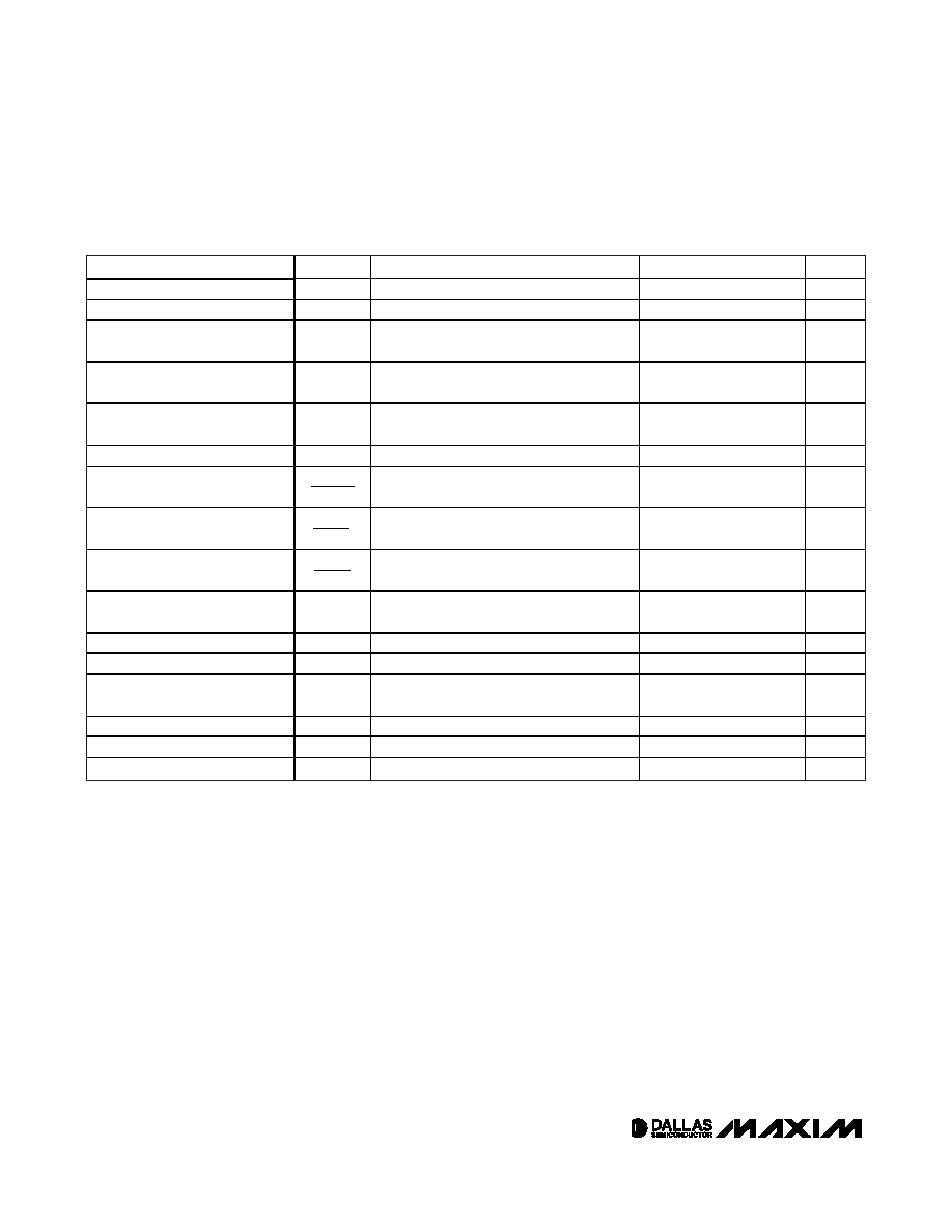
AC ELECTRICAL CHARACTERISTICS (DS1123L-100)
(VCC = +3.0V to 3.6V, TA = 0°C to +70°C.)
PARAMETER
SYMBOL
CONDITIONS
MIN
TYP
MAX
UNITS
Reference Delay
tREF
(Notes 3, 4)
18
22
ns
Delay Step Size
tSTEP
TA = +25°C
0
1
2.25
ns
Step-Zero Delay with Respect
to IN
tD0
(Notes 4, 5)
16.5
22
ns
Step-Zero Delay with Respect
to REF
tD0REF
(Notes 6, 7)
-2.5
-1.5
0
ns
Maximum Delay with Respect
to IN
tDMAX
(Notes 4, 8)
272
ns
Delay with Respect to REF
tDREF
Position FF (Notes 7, 9)
255
ns
Delay with Respect to REF
Tolerance
VCC = 3.3V, TA = +25°C
(Notes 7, 9)
-0.75
+0.75
%
Voltage Delay Variation
(Notes 7, 9)
-0.5
+0.5
%
Temperature Delay Variation
VCC = 3.3V (Notes 7, 9)
-2.5
+2.5
%
Integral Nonlinearity (Deviation
from Straight Line)
terr
(Note 10)
-4
0
+4
ns
OUT Delta Delay
tINV0
(Note 11)
0
1
2.5
ns
IN High to PWM High
tPWM0
(Notes 4, 12)
16.5
22
ns
Minimum PWM Output Pulse
Width
tPWM
(Note 13)
5
ns
Minimum Input Pulse Width
tWI
(Note 14)
40
ns
Minimum Input Period
(Note 15)
80
ns
Input Rise and Fall Times
tr, tf
(Note 16)
0
1
s
Note 1:
All voltages are referenced to ground.
Note 2:
If IN is high during power-up, the output remains low until IN is toggled low and back high again.
Note 3:
The reference delay is closely matched to the step-zero delay to allow relative timings down to zero or less.
Note 4:
Measured from rising edge of the input to the rising edge of the output (tDR).
Note 5:
Delay from input to output with a programmed delay value of zero.
Note 6:
This is the relative delay between REF and OUT. The device is designed such that when programmed to zero delay the
OUT output always appears before the REF output. This parameter is numerically equal to tD0 - tREF (see Figure 8).
Note 7:
From rising edge to rising edge.
Note 8:
This is the actual measured delay from IN to OUT. This parameter exhibits greater temperature variation than the relative
delay parameter.
Note 9:
This is the actual measured delay with respect to the REF output. This parameter more closely reflects the programmed
delay value than the absolute delay parameter (see Figure 8). Typical delay shift due to aging is within ±0.85%. Aging
stressing includes level 1 moisture reflow preconditioning (24hr +125°C bake, 168hr +85°C/85%RH moisture soak, and
three solder reflow passes +260°C +0°C/-5°C peak) followed by 1000hr (max) VCC biased +125°C OP/L, 1000hr unbi-
ased +150°C bake, and 1000 temperature cycles at -55°C to +125°C.
Δt
t
DREF
Δt
t
DV
DREF
Δt
t
DT
DREF
发布紧急采购,3分钟左右您将得到回复。
相关PDF资料
DS1124U-25+T
IC DELAY LINE 256TAP 10-USOP
DS1135LU-300/T&R
IC DELAY LINE 300NS 8-USOP
DS1135Z-12/T&R
IC DELAY LINE 12NS 8-SOIC
DS1181LE+
IC CLOCK MOD SS 8-TSSOP
DS1243Y-120
IC NVSRAM 64KBIT 120NS 28DIP
DS1244W-120IND
IC NVSRAM 256KBIT 120NS 28DIP
DS1248Y-70IND
IC NVSRAM 1MBIT 70NS 32DIP
DS1251WP-120+C02
IC NVSRAM 34PWRCP
相关代理商/技术参数
DS1123LE-200
功能描述:延迟线/计时元素 Programmable 3.3V 8 Bit Timing Element RoHS:否 制造商:Micrel 功能:Active Programmable Delay Line 传播延迟时间:1000 ps 工作温度范围: 封装 / 箱体:QFN-24 封装:Tube
DS1123LE-200+
功能描述:延迟线/计时元素 Programmable 3.3V 8 Bit Timing Element RoHS:否 制造商:Micrel 功能:Active Programmable Delay Line 传播延迟时间:1000 ps 工作温度范围: 封装 / 箱体:QFN-24 封装:Tube
DS1123LE-25
功能描述:延迟线/计时元素 Programmable 3.3V 8 Bit Timing Element RoHS:否 制造商:Micrel 功能:Active Programmable Delay Line 传播延迟时间:1000 ps 工作温度范围: 封装 / 箱体:QFN-24 封装:Tube
DS1123LE-25+
功能描述:延迟线/计时元素 Programmable 3.3V 8 Bit Timing Element RoHS:否 制造商:Micrel 功能:Active Programmable Delay Line 传播延迟时间:1000 ps 工作温度范围: 封装 / 箱体:QFN-24 封装:Tube
DS1123LE-50
功能描述:延迟线/计时元素 Programmable 3.3V 8 Bit Timing Element RoHS:否 制造商:Micrel 功能:Active Programmable Delay Line 传播延迟时间:1000 ps 工作温度范围: 封装 / 箱体:QFN-24 封装:Tube
DS1123LE-50+
功能描述:延迟线/计时元素 Programmable 3.3V 8 Bit Timing Element RoHS:否 制造商:Micrel 功能:Active Programmable Delay Line 传播延迟时间:1000 ps 工作温度范围: 封装 / 箱体:QFN-24 封装:Tube
DS1123LS-200
功能描述:延迟线/计时元素
RoHS:否 制造商:Micrel 功能:Active Programmable Delay Line 传播延迟时间:1000 ps 工作温度范围: 封装 / 箱体:QFN-24 封装:Tube
DS1123LS-25
功能描述:延迟线/计时元素
RoHS:否 制造商:Micrel 功能:Active Programmable Delay Line 传播延迟时间:1000 ps 工作温度范围: 封装 / 箱体:QFN-24 封装:Tube